

You are here
Back to topSurge Protection Components - TVS Selection
In high-reliability circuit design, mitigating transient voltages has become a crucial aspect of EMC design. Surge events are the primary cause of Electrical Overstress (EOS) in power components, often leading to system failure. This article first reviews the operating mechanisms of two protection components: TVS and MOV. It then further analyzes the key parameters of TVS and proposes practical selection considerations. By establishing these objective evaluation criteria, this guide aims to assist designers in selecting the optimal protection solution for diverse application environments.
Introduction
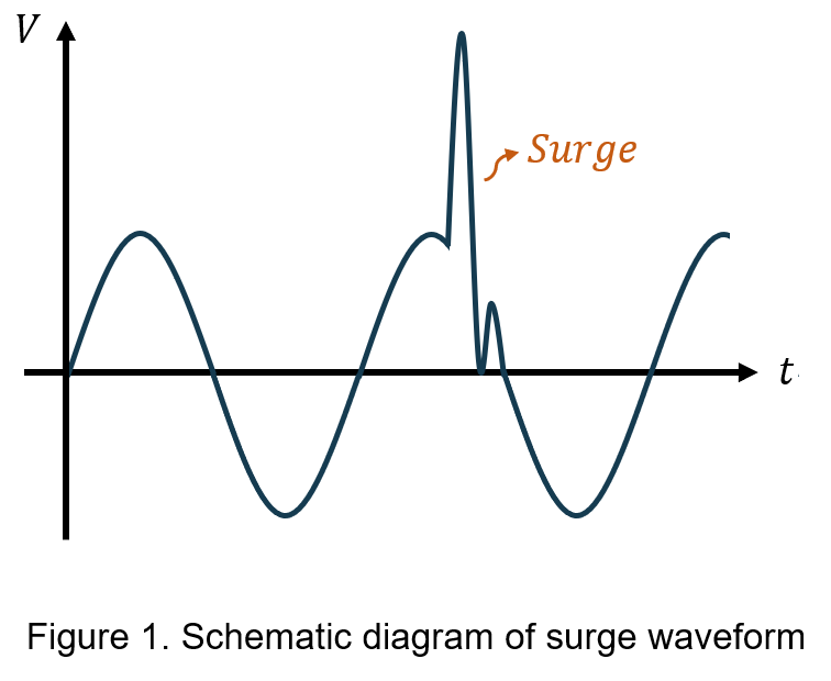
A surge refers to a high-energy, short-duration overvoltage event in a power system caused by lightning strikes or grid switching operations. As illustrated in Fig. 1, surge events are characterized by high voltage amplitude and substantial energy, distinguishing them from common switching transients or startup conditions.
The massive currents generated instantaneously can degrade the operational lifespan of power components, induce system malfunctions, and lead to data transmission distortion. For instance, grid-level surges often occur during the immediate restoration of power after an outage. In such scenarios, equipment housing high-precision PCBs—such as network switches or fire alarm control panels—is highly susceptible to internal short circuits or catastrophic hardware failure if the transient voltage exceeds the system's absolute maximum ratings.
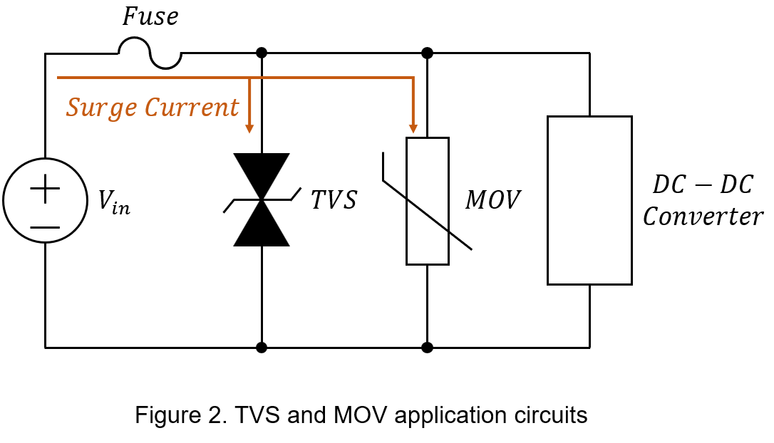
To mitigate these potential risks and comply with international immunity standards such as IEC 61000-4-5, circuit designs often incorporate surge protection components like TVS (Transient Voltage Suppressors) or MOV (Metal Oxide Varistors). The primary function of these devices is to provide a low-impedance path during an overvoltage event, shunting excess energy to ground and thereby safeguarding downstream ports and equipment. The following sections will examine the distinct characteristics of TVS and MOV surge suppressors, while also addressing the potential risks associated with a TVS device that fails to meet specific application requirements.
Exploring the Differences in Physical Characteristics Between TVS and MOV
In circuit protection design, both TVS and MOV are classified as voltage clamping devices. Unlike fuses that disconnect the circuit, these components transition rapidly into a low-impedance state during a transient overvoltage event, shunting excess energy to ground while limiting the downstream voltage to a safe level.
Despite sharing similar clamping characteristics, their underlying operating mechanisms differ significantly:
- TVS (Transient Voltage Suppressor): As a semiconductor-based device, it utilizes the avalanche breakdown effect to provide precise voltage clamping. Key advantages include picosecond-level transient response and excellent reliability (non-degrading) within its rated power limits. However, due to its lower peak power handling compared to MOVs, it is primarily used for secondary-side or signal-line protection.
- MOV (Metal Oxide Varistor): A ceramic nonlinear resistor characterized by extremely high energy absorption and surge current robustness, making it the preferred choice for primary-side protection at power inputs. However, MOVs suffer from irreversible thermal degradation after repeated surge events, leading to a progressive increase in leakage current over time. Consequently, long-term system reliability assessments must account for this aging mechanism and the associated safety risks
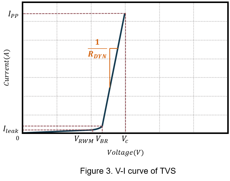
When comparing the two based on the same package size, we can observe the changes in their V-I curves at different voltages. Once the breakdown voltage is exceeded:
- TVS (Transient Voltage Suppressor): As shown in Figure 3, the V-I curve exhibits a sharp breakdown (hard knee). Due to its exceptionally low dynamic resistance (RDYN)
 , the clamping voltage (VC) remains tightly controlled within a precise range, even when subjected to high transient surge currents.
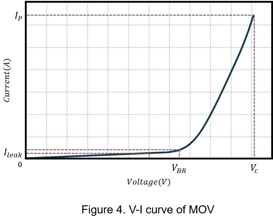
MOV (Metal Oxide Varistor): As shown in Figure 4, the curve features a more gradual or "soft knee" transition. Because its dynamic resistance(RDYN) ,is significantly higher than that of a TVS, the increase in clamping voltage (VC) becomes more pronounced under high-current surge conditions.
Peak power is generally considered as the product of the voltage and current limits on the curve:
- TVS (Transient Voltage Suppressor): The magnitude of the peak current is usually smaller, resulting in a generally lower overall peak power, making it suitable for the rapid protection of precision circuits.
- MOV (Metal Oxide Varistor): The peak current can reach thousands of amperes, significantly exceeding that of TVS, giving it a higher peak power load capacity that is suitable for high-energy surges.
In summary, while MOV has the advantage of a high energy carrying capacity, in high-speed communication power supply designs that demand rapid response and precise clamping voltages, the characteristics of TVS tend to be irreplaceable. To help optimize the protection design for sensitive components, the following section will provide an in-depth analysis of the key specifications of TVS.
Analysis of Key Electrical Parameters of TVS
In practical circuit design, component selection generally still relies on the specific parameters provided in the datasheet. The following aims to clarify the physical meaning of common parameters:
- Maximum Reverse Working Voltage(VRWM) : The safe upper voltage limit at which the device maintains an extremely low leakage current.
 VRWM should generally be higher than the expected maximum operating voltage of the system; if the applied voltage exceeds VRWM, it might lead to a significant increase in leakage current. For example, if the maximum input voltage of a power module is 24V, a TVS with a VRWM of at least 24V should be selected.
 - Breakdown Voltage(VBR)
 : This is the threshold at which the TVS diode begins to conduct, typically defined at a leakage current of 1mA. Once the voltage across the device exceeds
  VBR, the leakage current increases exponentially (the diode "turns on"). Due to the potential shift in VBR , caused by manufacturing process variations and temperature, it is critical to ensure that the nominal system operating voltage remains below VBR rather than
  to guarantee ultra-low leakage.
 - Clamping Voltage(VC)
 : The maximum voltage to which the two terminals of the TVS are limited when surge current occurs. Its calculation formula is:
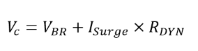
Where ISurge is the surge current, and RDYN is the internal equivalent resistance after the component conducts, which determines the slope of the V-I curve. The voltage stress encountered during a surge generally depends on VC. By reducing VC, the margin between the protection voltage and the component's withstand voltage limit can be effectively increased, which can significantly reduce the probability of damage caused by electrical overstress (EOS). In other words, VC should be controlled below the withstand voltage limit of the protected circuit; if VC exceeds this threshold, the residual overvoltage may still cause junction breakdown or permanent damage to sensitive components, even if the protection device is actively shunting current. - Leakage Current Ileak : This is the minute current that flows through the device when the normal operating voltage is applied. During selection, choosing a device with excessive Ileak will lead to unnecessary power consumption and reduced battery life in portable applications.
- Peak Pulse Current (IPP)
: This represents the maximum surge current a TVS diode can withstand without suffering thermal failure. It is a critical parameter for determining whether a device has sufficient energy absorption capacity; therefore, its rated value must exceed the system's expected peak surge current. If the IPP rating is too low, excessive surge energy may cause thermal damage or catastrophic breakdown of the TVS itself, leading to a total loss of protection for downstream stages. - Parasitic Capacitance(Cin)
: This is the equivalent internal capacitance of the TVS diode. In high-speed signal applications, excessive capacitance can form a low-pass filtering effect with the transmission line, resulting in high-frequency signal attenuation and distortion.
Conclusion
In hardware protection circuits, overvoltage protection design should generally be based on the energy level and response requirements of the application. MOVs are well-suited for handling high-energy transients at the power input stage, while TVS devices, with their ultra-low dynamic resistance and fast response time, provide more precise and rapid voltage clamping under transient conditions. This makes TVS particularly suitable for protecting sensitive components with limited voltage margin.
The key to a successful protection design usually lies in "precise component selection." First, VRWM should generally be higher than the system's maximum operating voltage to prevent excessive leakage current. Second, VC must remain below the absolute maximum voltage ratings of the downstream circuitry to effectively prevent surge-induced damage. Simultaneously, IPP should also be higher than the actual peak surge current that might occur, ensuring that the component does not fail due to thermal overload. Furthermore, in high-speed signal applications, parasitic capacitance must be maintained within a reasonable range to avoid compromising signal integrity. By comprehensively evaluating these parameters, engineers can establish a robust and stable protection architecture.
CTC is service provider for high-end power modules (DC to DC Converter and AC to DC Converter) for critical applications worldwide since 1987. We aim to be business generator and a virtual business unit. CTC is your own team with 35 years of experience for a strong business program from market research, product definition & development, supply chain management and total technical services.
CTC is the only corporation certificated with ISO-9001, IATF-16949, ISO22613(IRIS), and ESD/ANSI-2020. We can 100% ensure not only the product, but also our workflow and service to match quality management system for every high-end application from the very beginning. From design to manufacturing and technical support, every single detail is operated under highest standard.