

You are here
Back to topPoE PD Power Topology and Layout Design
With the rapid growth of the Internet of Things (IoT), Power over Ethernet (PoE) has become an increasingly important power delivery method for end devices. However, designing highly reliable PoE Powered Devices (PDs) still involves significant challenges, particularly in meeting wide input voltage ranges and broad power requirements. This application note describes a PoE power architecture compliant with the IEEE 802.3 standard and focuses on two key design aspects of the internal DC-DC converter in the PD: topology selection and hardware implementation. For different end-device power levels, this note analyzes the suitability of various topologies and further presents layout and thermal management considerations for high-power applications to enhance long-term system reliability.
Introduction
Power over Ethernet (PoE) technology enables both data and power to be transmitted over a single Ethernet cable, greatly simplifying cabling for end devices. In practical applications, power requirements vary widely, ranging from micro-sensors that consume only a few watts to multi-sensor edge devices that require tens of watts. This wide power range places significant demands on the flexibility and stability of the internal power design.
In a typical PoE network, the system primarily consists of Power Sourcing Equipment (PSE) and Powered Devices (PD). In practice, the physical connection architecture is mainly divided into two types: the Endspan PSE architecture, where power is directly supplied by a PoE-enabled network switch, and the Midspan PSE architecture, where an additional PoE Injector is connected in series between a traditional switch and the PD, as shown in Figure 1.
![]()
Regardless of the architecture used, once power is transmitted to the PD, it enters the internal pure power conversion path to provide stable voltages for various system units. To ensure compatibility and safety across equipment from different manufacturers, IEEE has established the rigorous 802.3 series of standards, classifying PoE devices into Type 1 to Type 4 based on their power capabilities, as shown in Table 1.
| IEEE Standards | PSE Maximum Output Power | PD Maximum Available Power | |
| Type 1 | IEEE 802.3af | 15.4W | 13.0W |
| Type 2 | IEEE 802.3at | 30.0W | 25.5W |
| Type 3 | IEEE 802.3bt | 60.0W | 51.0W |
| Type 4 | IEEE 802.3bt | 90.0W | 71.3W |
This application note will explore how to select DC-DC converter topologies based on power requirements, and provide specific layout and thermal management strategies to build highly efficient and reliable PoE terminal devices.
PoE System Architecture and Pre-design Considerations
(1) PoE System Architecture
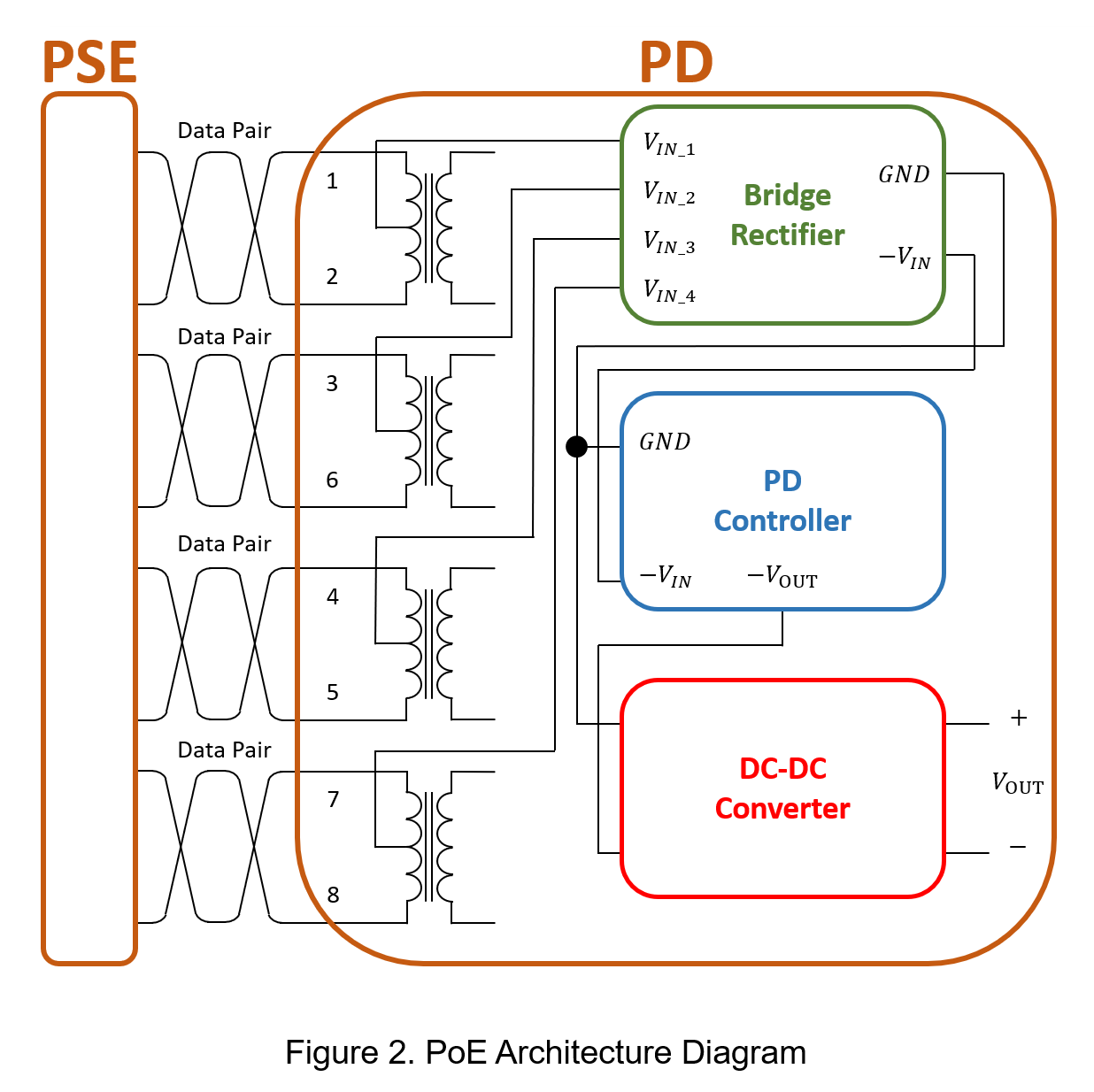
PoE technology delivers both data and power over a single Ethernet cable. After power enters the PD, the 48V DC is taken from the center tap of the Ethernet transformer, then passes through a bridge rectifier and the PD interface controller before being fed into the DC-DC converter for step-down conversion. Figure 2 omits the internal data communication path within the PD and shows only the power-processing architecture of the PSE, the data pairs, and the PD side.
(2) Design Challenges
Focusing on the core design of the DC-DC converter, two major challenges of the PoE system must first be overcome:
Challenge 1: Wide Input Voltage
During long-distance transmission over Ethernet cables, voltage drop occurs due to the cable’s DC resistance. Aging connectors can further increase contact resistance, while heat buildup may introduce additional thermal stress and losses. As a result of these factors, the input voltage reaching the PD can fall below 37V. When output power remains constant, a lower input voltage leads to a higher input current  . Based on the conduction loss equation of the switching device:
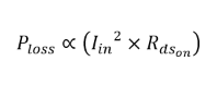
Because conduction loss is proportional to the square of the current, any increase in input current causes switching losses and power dissipation to rise rapidly. This in turn increases device temperature and becomes a key limitation in high-power PoE design.
Challenge 2: Wide Range of Output Power
PoE devices cover a broad range of power levels. If a high-power device uses a converter topology intended only for light-load operation, excessive voltage stress and thermal issues may occur under heavy load. Conversely, if a low-power device uses an overly complex high-power architecture, unnecessary hardware cost will result. Therefore, selecting the appropriate converter topology according to the target power level is critical to balancing performance and cost.
DC-DC Converter Topology Selection
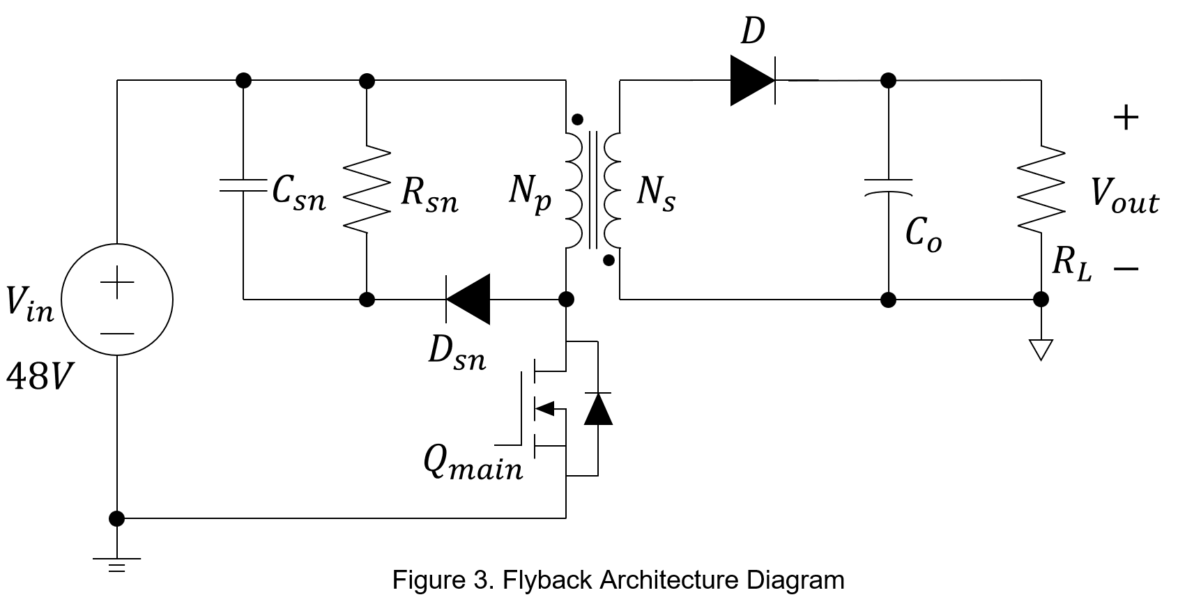
To balance conversion efficiency, development cost, and thermal performance, hardware design should follow the principle of proper power matching. The most common converter topology for PoE PDs is the flyback topology, as shown in Figure 3. It is widely used for three main reasons:
- Simple Structure: Its streamlined architecture offers excellent cost-effectiveness.
- Inherent Isolation: It provides natural galvanic isolation, making it easier to meet PoE safety requirements.
- Wide Input Suitability: It can accommodate a wide input voltage range, making it well suited to handle voltage fluctuations caused by long Ethernet cable runs.
As PoE power requirements increase to Type 3 and Type 4 levels, the traditional flyback topology suffers from higher conduction and switching losses under high-current conditions, which limits its ability to scale to higher power levels. To address this issue, high-power PoE designs can adopt the Active Clamp Flyback (ACF) topology, as shown in Figure 4. By using resonant operation to achieve zero-voltage switching (ZVS), ACF can effectively reduce the losses and heat generation associated with high-frequency switching.
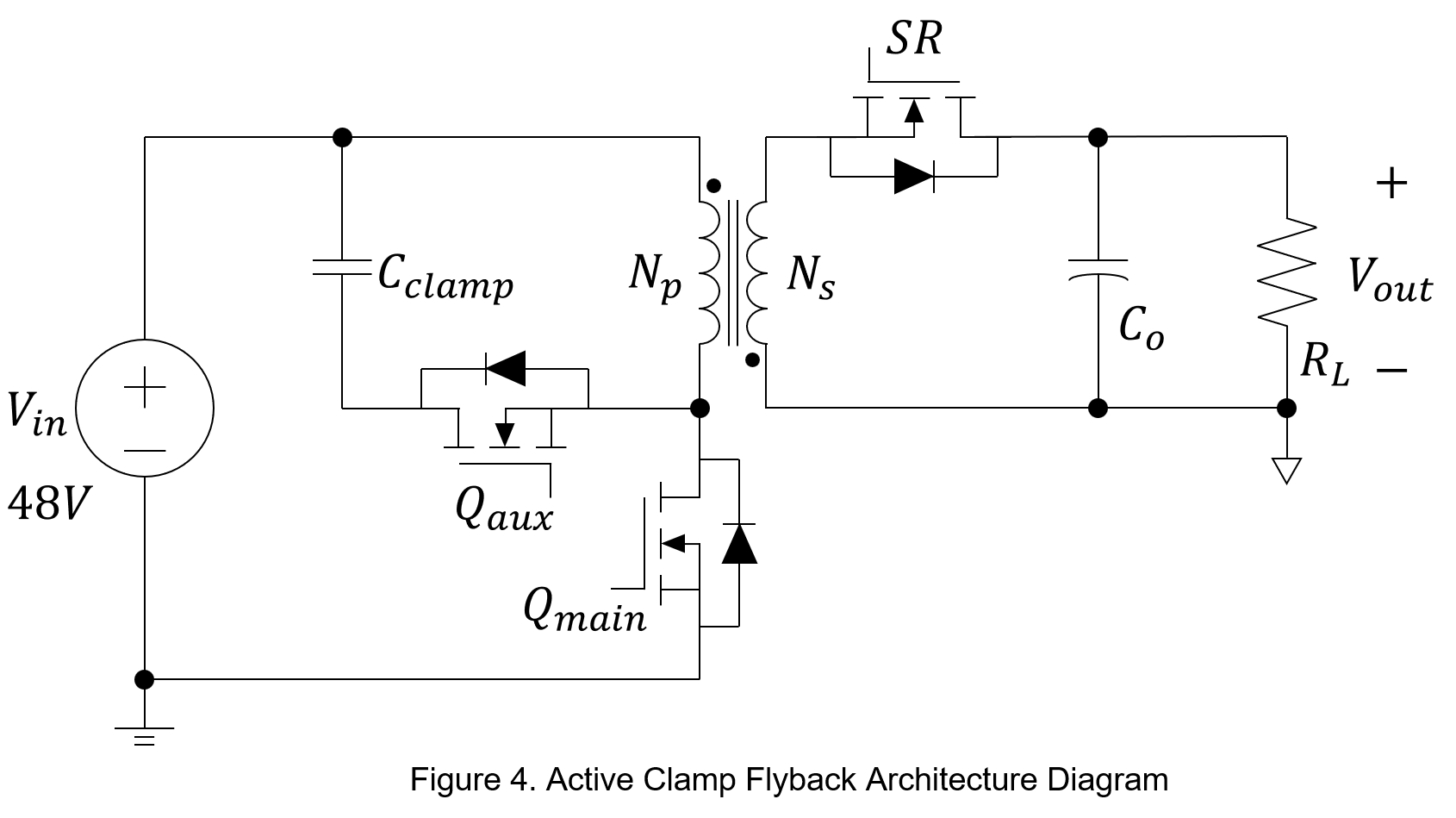
However, ACF controllers typically come with higher cost, and their control loop design is more complex. Considering mass production and system reliability, high-power PoE designs that require improved efficiency often favor the simpler flyback topology, combined with the following two approaches to reduce heat generation:
- Synchronous Rectification (SR): Conventional diodes introduce significant forward voltage drop losses (typically 0.6–0.8 V). Replacing them with low-on-resistance MOSFETs significantly reduces conduction losses and heat generation under high current conditions.
- Low-Resistance ( Rds_on)
witching Components: Using MOSFETs with low on-resistance for both primary- and secondary-side switching helps minimize conduction losses under high current operation.
Through these optimizations at both the component and topology level, thermal stress in high-power designs can be reduced without significantly increasing control complexity. This enables a more efficient and cost-effective solution for high-power PoE applications.
Practical Design and Thermal Management Strategies
Under high-current operating conditions, the transformer and PCB trace impedances, which are highly critical in Flyback designs, become the main sources of thermal loss. Therefore, physical design is the key to determining the system's ultimate performance and long-term reliability.
(1) Magnetic Component Cooling: Planar Transformers
When the converter enters high-power and high-frequency applications, traditional wire-wound transformers will face the following heat generation issues:
- Leakage Inductance: Poor coupling of the enameled wire windings generates substantial leakage inductance. The stored energy is converted into waste heat by the snubber circuit.
- Core Loss: High-frequency operation increases the hysteresis loss and eddy current loss of the magnetic core.
- Skin Effect: High-frequency alternating currents are pushed to the surface of the copper wire, drastically reducing the effective conductive cross-sectional area and causing the AC resistance (Rac)
 to surge non-linearly. The formula for the skin depth is:
4. Proximity Effect: The electromagnetic fields between densely packed multi-layer windings interfere with each other, further exacerbating the uneven current distribution.
To solve the heat dissipation and loss bottlenecks of traditional Flyback converters at high frequencies and high power, Planar Transformers can be used to replace traditional transformers. A comparison of the two is shown in Table 2:
| Traditional Wire-wound Transformer | Planar Transformer | |
| Winding | Round enameled copper wire | Flat copper foil inside multi-layer PCB |
| AC Impedance | High | Low |
| Leakage Inductance | High | Low |
| Heat Dissipation | Poor | Good |
| Core Loss | High | Low |
| High-Frequency Application | Poor | Good |
(2) PCB Layout: Parasitic Parameter Suppression and Heat Conduction
Frequent switching of high currents results in high di/dt and dv/dt on the PCB, increasing switching losses and heat generation. For high-power PoE systems, the following layout guidelines should be considered:
- Minimize Main Current Loop: The primary current loop in a flyback topology should be kept as compact as possible. Reducing loop area directly lowers parasitic inductance (Lparastic) , thereby reducing voltage stress and associated losses in the main switching MOSFET.
- Optimize Switching Node Copper Area: The drain copper area of the main switching MOSFET should be carefully sized to balance current-carrying capability and parasitic capacitance to ground. Excessive copper area can increase capacitive coupling and high-frequency noise injection into the system ground. Sensitive signal traces should be routed away from this node, including adjacent areas on the same layer as well as directly above or below it, to minimize noise coupling caused by high dv/dt.
- Thermal Via Design: The thermal performance of surface-mount devices (SMDs) depends heavily on PCB heat conduction. Placing an array of thermal vias beneath the device’s thermal pad enables efficient vertical heat transfer to inner layers or large ground planes, helping to reduce localized heat buildup and hot spots.
Conclusion
As PoE technology continues to advance from early low-power implementations to IEEE 802.3bt Type 3 and Type 4 high-power applications, PD power designs face increasingly demanding requirements for efficiency, thermal performance, and long-term reliability. To accommodate input voltage variation caused by long cable runs and a broad range of end-device power levels, designers must balance converter topology, component selection, and PCB implementation. In practice, the flyback topology remains the preferred solution for many PoE PD designs. By adopting synchronous rectification, low-Rds(on) MOSFETs, and high-efficiency magnetic components, designers can improve conversion efficiency and reduce thermal stress in high-power operation. Equally important, proper PCB layout and sound thermal management are critical to achieving reliable long-term system performance.
CTC is service provider for high-end power modules (DC to DC Converter and AC to DC Converter) for critical applications worldwide since 1987. We aim to be business generator and a virtual business unit. CTC is your own team with 35 years of experience for a strong business program from market research, product definition & development, supply chain management and total technical services.
CTC is the only corporation certificated with ISO-9001, IATF-16949, ISO22613(IRIS), and ESD/ANSI-2020. We can 100% ensure not only the product, but also our workflow and service to match quality management system for every high-end application from the very beginning. From design to manufacturing and technical support, every single detail is operated under highest standard.