

You are here
Back to topConsiderations for Placing Input Capacitors
For noise-sensitive circuits, using multiple capacitors with different values in parallel can enhance high-frequency noise attenuation, suppress rapid voltage fluctuations, and improve feedback loop stability. To optimize filtering performance, it is essential to select capacitor values based on the target noise frequency range and to place the capacitors properly. This article discusses key considerations and precautions related to the placement of input capacitors in PCB layouts.
Introduction
When designing a DC-to-DC converter, selecting the correct circuit topology and appropriate components is crucial. As one of the key components on the PCB, the input capacitor serves the following main functions:
(1) Filtering: The input capacitor effectively suppresses high-frequency noise on the input voltage, providing the DC-DC converter with a stable input source and reducing electromagnetic interference (EMI).
(2) Energy Storage: When the load current suddenly increases, the input capacitor can quickly deliver additional current to meet the demand, thereby improving the converter’s transient response.
(3) Protection: During power-on or power-off transitions, the input capacitor absorbs inrush current, protecting the internal components of the converter.
(4) Impedance Matching: The input capacitor improves the input impedance characteristics, reducing the converter’s impact on the power supply and enhancing overall system stability.
Therefore, understanding how to properly lay out all components is equally important. Improper placement of input capacitors can result in excessive conducted or radiated noise, increased PCB area, higher electromagnetic interference (EMI), and even system instability during load transients. This article compares the advantages and disadvantages of different capacitor types across various capacitance values and discusses considerations for optimal placement. By planning component placement in advance, designers can enhance the performance, stability, and reliability of their products.
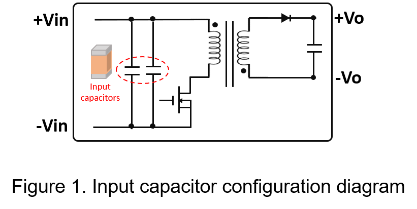
Input capacitor configuration arrangement
When an isolated converter operates in boost mode, the input capacitor must handle significant current depending on the input-to-output voltage ratio, and large instantaneous ripple currents can occur during high-frequency switching. As a result, the input capacitor is subjected to rapid and repetitive high-current stress. Converters often employ large-value aluminum electrolytic capacitors to store sufficient charge, preventing voltage droop during load transients and attenuating low-frequency noise. However, aluminum electrolytic capacitors exhibit poor high-frequency characteristics and relatively high energy loss. Therefore, surface-mount multilayer ceramic capacitors (MLCCs) with low equivalent series resistance (ESR) and low equivalent series inductance (ESL) are used for high-frequency decoupling.
Using multiple capacitors of different values in parallel provides better noise attenuation, as the overall attenuation curve begins at the first pole and ends at the final zero. Theoretically, the largest capacitor value determines the start frequency of attenuation, while the smallest determines the end frequency. Therefore, paralleling a large-value aluminum electrolytic capacitor with a small-value MLCC enables effective filtering across both low- and high-frequency ranges.
A key design consideration is how to arrange these two capacitors along the primary current path. The input capacitor should be the first component in the PCB layout. After placement, the connection path to the converter must remain free of any intervening components. To minimize parasitic inductance, the input capacitor should be positioned as close as possible to the converter’s input pins, on the same PCB layer, and connected using wide and short traces with a minimized ground return loop.
In practical designs, the input supply is typically decoupled first by a large capacitor, Cin1 (e.g., 10 µF), followed by a smaller capacitor, Cin2 (e.g., 0.1 µF), before reaching the converter’s transformer or power switch, as illustrated in the figures below.
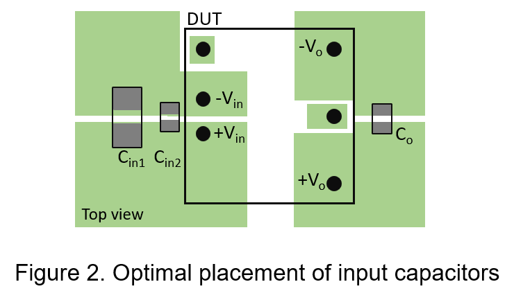
Figure 2 illustrates the input capacitor placed in close proximity to the converter’s input pin, ensuring a direct connection without any intervening components. This placement minimizes the current loop area.
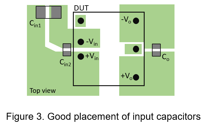
In Figure 3, the large-value capacitor is positioned farther from the converter, but there are no intervening components along the connection path. Nevertheless, it is recommended to place the input capacitor as close to the converter’s input pin as possible to achieve optimal performance.
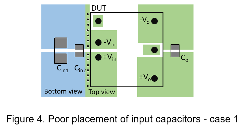
In Figure 4, the input capacitor is placed on the backside of the PCB and connected to the converter’s input pin through vias. This configuration increases the trace impedance due to the additional resistance and inductance introduced by the vias, which can degrade the input voltage transient response and potentially cause voltage droop during high-current startup.
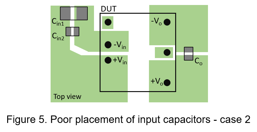
In Figure 5, the large loop area formed between the multilayer ceramic capacitor and the input pin is susceptible to high-frequency noise coupling, which can lead to increased electromagnetic interference (EMI).
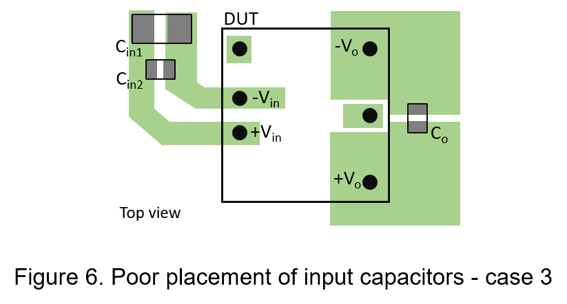
As shown in Figure 6, the trace connecting the input capacitor to the input pin should be short and wide to prevent current crowding. Using wide copper planes or a solid ground plane helps lower the impedance of the return path and reduces noise coupling.
Experimental Result
This experiment was conducted to evaluate the impact of PCB trace and via inductance on input signal integrity. An isolated DC-DC converter was used to examine the effect of input capacitor placement distance. Measurements were taken using a short ground probe at two test points: C1, located adjacent to the input capacitor, and C2, located adjacent to the DC-DC converter, approximately 20 mm apart, as illustrated in the figure.
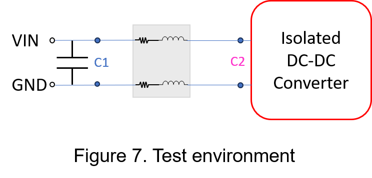
| Input voltage | 24Vdc |
| Output voltage/current | 12 Vdc / 2.5A |
| Operating frequency | 400kHz |
| Ripple & noise | 750mVp-p (max) |
The experimental results are as follows:
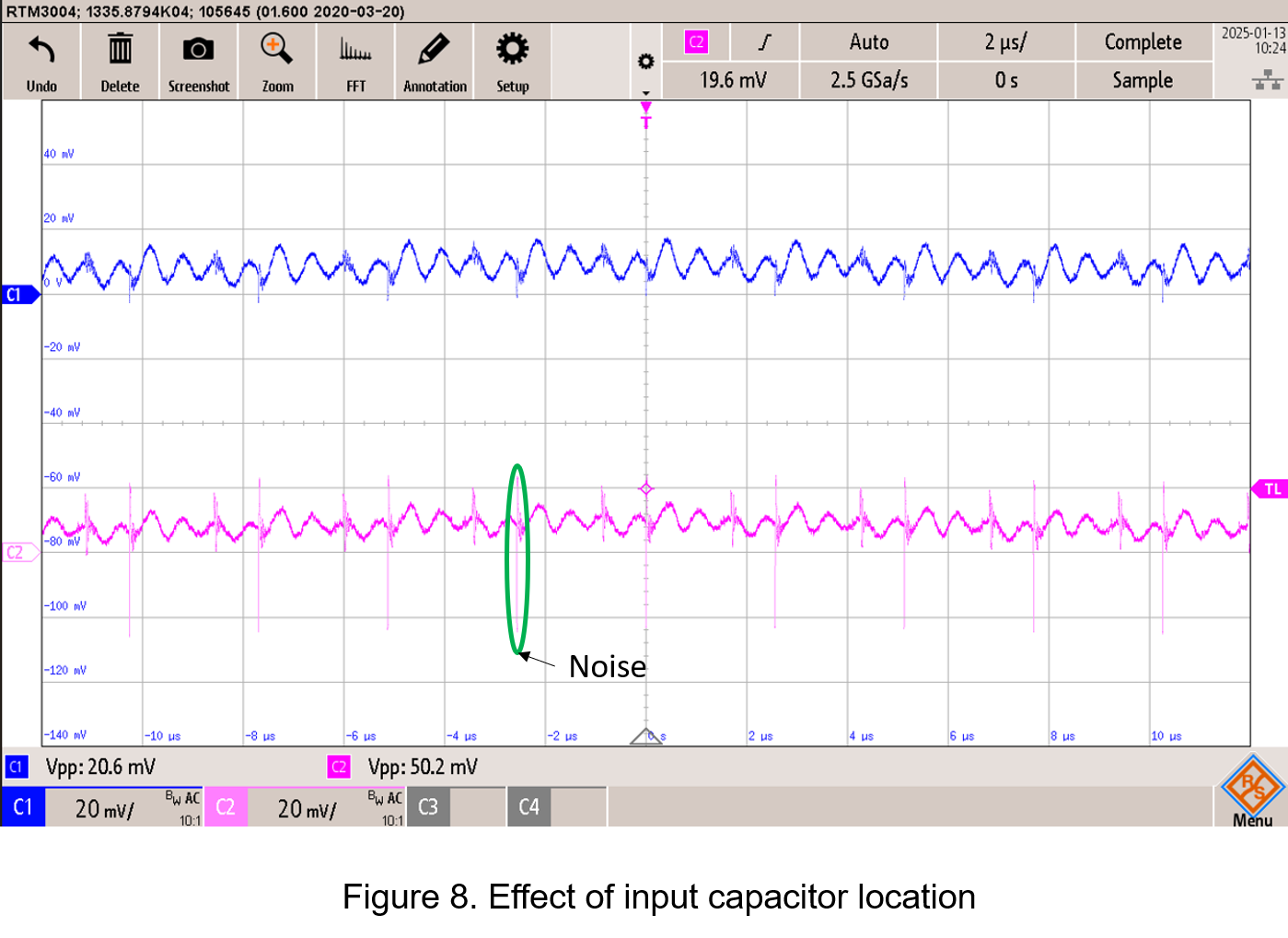
The measurement results indicate that increasing the distance from the input capacitor leads to a significant rise in voltage ringing. The test point closest to the input capacitor exhibited a peak-to-peak voltage of 20.6 mV, compared to 50.2 mV at the more distant point, representing more than twice the ringing amplitude.
Conclusion
For circuits that are susceptible to input noise, the placement of the input capacitor on the PCB is a critical design consideration. To mitigate noise and improve electromagnetic compatibility (EMC), the input capacitor should be positioned carefully. Reducing the distance to the converter, widening the input traces, and minimizing unnecessary layer transitions are effective strategies to suppress noise, provide a cleaner input supply, and enhance overall power integrity.
CTC is service provider for high-end power modules (DC to DC Converter and AC to DC Converter) for critical applications worldwide since 1987. We aim to be business generator and a virtual business unit. CTC is your own team with 35 years of experience for a strong business program from market research, product definition & development, supply chain management and total technical services.
CTC is the only corporation certificated with ISO-9001, IATF-16949, ISO22613(IRIS), and ESD/ANSI-2020. We can 100% ensure not only the product, but also our workflow and service to match quality management system for every high-end application from the very beginning. From design to manufacturing and technical support, every single detail is operated under highest standard.