

You are here
Back to topHow do you reduce voltage ripple?
Introduction
- Ripple Voltage
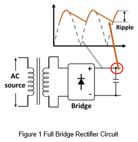
Ripple voltage means the amount of AC voltage that appears on a DC voltage. The main reason for the ripple voltage is that the converter converts the AC voltage into a DC voltage, but the AC voltage cannot completely eliminate. For example, Figure 1 is a schematic diagram of a full bridge rectifier with a capacitor connected to the output side. The dotted line is the voltage waveform before full bridge rectifier, the solid line is the voltage waveform after capacitor filtering, and the ripple voltage refers to the peak-to-peak value of the solid line.
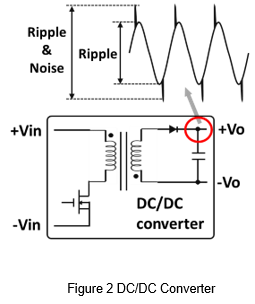
The ripple voltage shown in Figure 1 is low frequency ripple voltage. In higher frequency applications, such as AC to DC or DC to DC converters, the frequency of the ripple voltage maybe be higher. Figure 2 is a schematic diagram of a DC/DC converter. The voltage noise is generated during the MOSFET switching and coupled to the output side through the transformer. And finally the ripple measured at the output capacitor is a ripple voltage that contains noise components.
- Measurement Methods
The general method of measuring voltage is to use a voltage probe to measure the output or load side as shown in Figure 3. And display the volume of the output voltage through an oscilloscope. However, if used the same methods to measure the ripple voltage, the waveform is susceptible to interference.
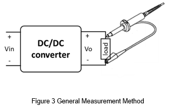
Figure 4 shows the ripple voltage measured using a general measurement method. It can be seen that the noise part is significantly higher. This is mainly due to the long ground wire of the probe. The measurement path for the probe is equivalent to the increase of parasitic inductance, which causes noise in the output voltage waveform. This is not caused by the converter, and it is easy for misjudgment. So, the correct measurement method is very important.
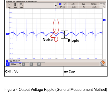
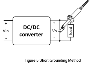
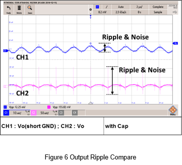
Figure 5 shows the correct ripple measurement method. It can be seen from the figure that the output of the converter is connected with a filter capacitor. The purpose is to suppress noise, so the capacitor value is usually not too large, mostly at 0.1uF to 1uF. And the probe should use a short grounding method for measurement. The measure point should change from the load to the output capacitor. The purpose is to avoid measuring noise. Figure 6 shows the difference between the ripples of short ground and no short ground. The ripple voltage of the converter can be measured correctly if used the right methods.
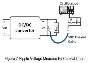
Most ripple voltage measurements are when the oscilloscope is close to the converter. If the distance is relatively long, it may not be suitable to use a voltage probe for measurement. The more suitable method is to use a 50Ω BNC connector and a coaxial cable for long-distance measurement, as shown in Figure 7. It should be noted that the shorter the cable length from the output end of the coaxial cable to the capacitor and the oscilloscope, the less likely it is to receive interference.
This article is using voltage probe and short ground method and used 20MHz bandwidth to measure the ripple voltage.
External Circuit For Reduce Ripple & Noise
The following will list four external circuit and explain the theory for the schematic.
- Capacitor
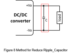
As shown in Figure 8, Connecting a capacitor to the output of the converter is a simple way to reduce the output voltage ripple.
Take full bridge converter as an example.
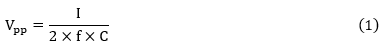
Vpp is the peak-to-peak value of the ripple voltage.
I is the output current.
f is the operating frequency.
C is the capacitance.
As shown in formula (1), the ripple voltage is inversely proportional to the capacitance. That is, the larger the capacitance, the smaller the ripple voltage. Which shows that the external capacitor helps to suppress the ripple voltage.
- Low Pass Filter
A low pass filter maybe a good chose to reduce the ripple voltage more than a capacitor, as shown in Figure 9.
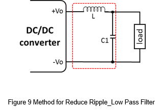
It can used frequency response to calculate the parameters of L and C.
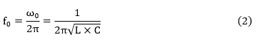
f0 is Cutoff frequency.
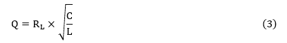
Q is Quality factor.
RL is Output load.
Take formula (3) into formula (2), and it can calculate the L and C respectively, as shown in formula (4) and (5).
![]()
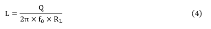
The quality factor is related to the load impedance and the LC filter, which can be divided into three curves of over damping, critical damping and under damping, as shown in Figure 10. Ideally, the use of critical damping as the parameters of the LC filter is most suitable.
- Common Mode Choke Filter
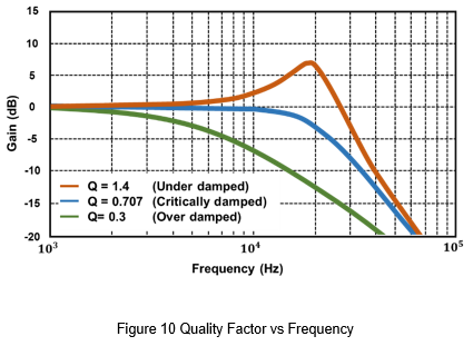
Due to there has some switching components inside the converter, and it will generate switching noise. These noises may also be transmitted to the output side. And the common mode choke filter can limit this kind of noise, as shown in Figure 11.
Common mode choke filter is commonly used as an EMI filter. However, there is still leakage inductance inside the common mode filter. The leakage inductance act as a differential mode inductor, and it similar as the LC rate filter. So, the common mode filter inductor can still have some effect on ripple voltage suppression.
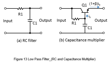
- Capacitance Multiplier
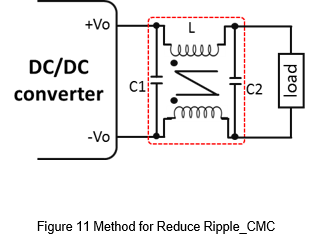
Figure 12 shows the capacitance multiplier circuit, and it can reduce the output ripple by transistor and R, C. For the output side, it has the effect of amplifying C1, similar as add a large capacitance at the output side. It is suitable for need to reduce ripple voltage and have size limit application.
As shown in Figure 13 (a), it is a RC low-pass filter in the circuit. If want to suppress the voltage ripple, the capacitance of C1 must be very large. If a transistor is added to this, as shown in Figure 13(b), the current supplied by C1 to the output is about β times down. In other words, the capacitance of C1 is amplified by about β times to the output.
The capacitance multiplier circuit also has disadvantages, because the voltage of the transistor Vce will change with the output current, which will cause a certain voltage drop at the output side, the range maybe from 0.65V to 3V. Therefore, this is suitable for small current application and the voltage accuracy is not high, such as an OP amplifier or a DAC power supply.
Application
In the following, a specific DC-to-DC converter will be used to measure the difference in ripple voltage before and after through different ripple voltage reduce circuits.
The converter is a wide input voltage range from 9 to 36V input, 5V output regulated converter, the output power is 30W, the output current is 6A, the specifications are shown in Table 1.
| DC to DC Converter | PF30WR4-2405 |
| Input voltage | 24 Vdc |
| Output | 5 Vdc / 6A |
| Operating frequency | 400kHz |
| Ripple & noise | 75mVp-p (max) |
- Capacitor
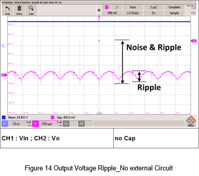
Figure 14 shows the voltage ripple waveform of output by using a short ground method. Due to there are no additional noise suppression circuit. It can be seen that the peak-to-peak value of the output voltage ripple and noise is about 445.9mV when there is no external capacitor.
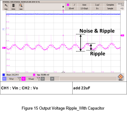
In order to suppress the output voltage ripple and noise, the most common and simple way is add the capacitor.
Figure 15 shows the output voltage ripple measured by an external 22uF MLCC. From the figure, the ripple voltage reduced from 445.9mV to about 30mV.
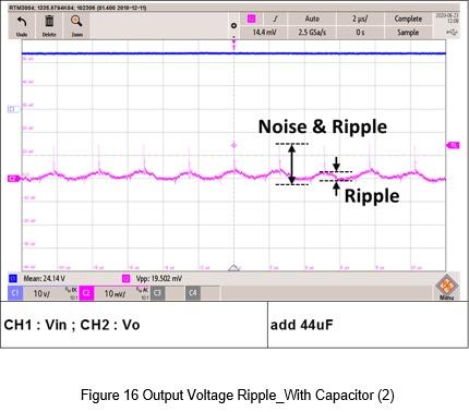
In addition, Figure 16 show the waveform for double the output capacitor. The output voltage ripple becomes lower and the peak-to-peak value is 19.5mV. Therefore, an external capacitor at the output of the converter can effectively suppress the output voltage ripple.
- Low Pass Filter
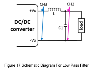
Fig. 17 is a schematic diagram of a low-pass filter. From the converter specification table, the converter operating frequency is 400kHz. First set the cut-off frequency to 40kHz and the quality factor to 0.707. Through equations 4 and 5, it can get the inductance is 4.69uH and the capacitance is 3.376uF. Finally choose 4.7uH inductance and two 2.2uF MLCC as the output low-pass filter.
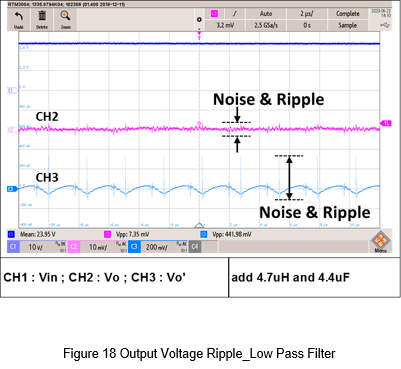
Figure 18 is a waveform of the output voltage ripple. There is a comparison before and after filter. The low-pass filter, the ripple and noise are effectively suppressed.
- Common Mode Choke Filter
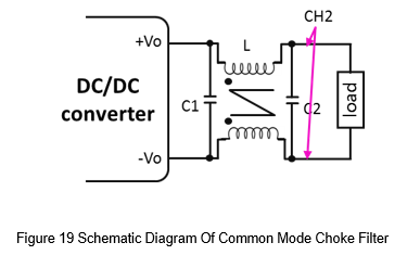
Figure 19 is a schematic diagram of common mode choke as an output filter. In this experiment, a Mn-Zn ferrite core of A151, T16x12x8C used as an iron core. The number of windings is 10. The main inductance is 0.35mH, and the leakage inductance is 3.18uH. C1 and C2 is 0.22uF MLCC.
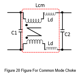
Figure 20 is a schematic diagram of a common mode filter. It can be seen that the leakage inductance is used as a differential mode inductance, which is the same as two low-pass filters, so the output voltage ripple suppression effect should better than single low-pass filter.
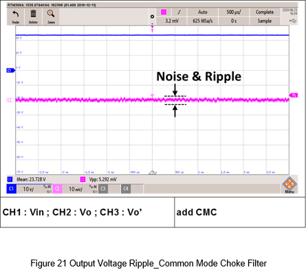
Figure 21 is the measure waveform. It is true that the ripple voltage is lower than single low pass filter, but the disadvantage is that it takes more layout space.
- apacitance Multiplier
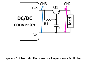
Figure 22 shows the schematic diagram of this experiment, the parameters are as follows.
Q1 is 2SCR552PT100, it is a transistor of ROHM.
R1 is 1kΩ.
C1 is 4.7uF.
Since the capacitance multiplier is suitable for low power or signal level. Because it will cause voltage drop, it is not suitable for high current applications. So, the output current of this experiment is limited to 0.2A.
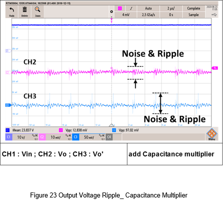
Figure 23 is the test waveform. It can see the difference between before and after filter. The ripple before suppression is about 97mV and the ripple after suppression is 12.8mV, which can reduce the voltage ripple. The disadvantage is that it can only be used in signal level, instant of higher output power.
Conclusion
This article has introduction about the formation of ripple and noise, and the measurement method. Also provides four kinds of ripple and noise reduction methods, and do the experiment for each kind of filter.
Table 2 shows the comparison table for the four methods, the lower the score the better.
From the overall score, only the addition of capacitors is the most suitable ripple suppression method, which not only has the smallest volume but also has a certain effect.
The second and third are low pass filter and common mode filter. Because it has external inductors and common mode choke, the layout space is larger than capacitor, but the effect is better. Therefore, many low ripple applications are used these two methods.
The fourth is the capacitance multiplier circuit, which has a good effect on the suppression of ripple voltage, but it can only be used for low current or signal level, which limits the application.
| C | LC filter | CMC filter | C multiplier | |
| Part count | 1 | 2 | 3 | 3 |
| Layout space | 1 | 2 | 3 | 3 |
| Ripple & Noise suppression | 2 | 1 | 1 | 1 |
| Output current | 1 | 1 | 1 | 3 |
1→Good, 2→Middle, 3→Poor
CTC is a professional service provider for high-end power supply modules (AC to DC Converter and DC to DC Converter) for critical applications worldwide since 30 years. Our core competence is to design and deliver products with leading technologies, competitive pricing, extremely flexible lead-time, global technical service and high-quality manufacturing (Made In Taiwan).
CTC is the only corporation certificated with ISO-9001, IATF-16949, ISO22613(IRIS), and ESD/ANSI-2020. We can 100% ensure not only the product, but also our workflow and service to match quality management system for every high-end application from the very beginning. From design to manufacturing and technical support, every single detail is operated under highest standard.