

You are here
Back to topRequirements of Isolated Gate Driver Power
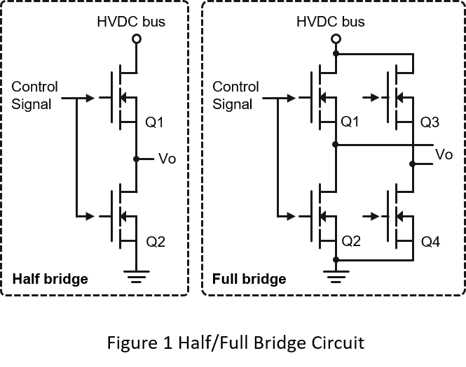
There are commonly used half bridge or full bridge topology, in high power AC/DC converter or DC/AC inverter application as Figure 1 shows. This topology commonly used IGBT and MOSFET, SiC and GaN as switching elements. And if the application is high voltage inverter for Motor driver, the high side IGBT/MOSFET need isolated driver and power.
In addition, the gate driver and the gate driver power need have low isolation capacitors to prevent leakage current from causing temperature rise. And prevent mis-operation of switching element cause by noise. Also, in motor drive applications, the insulation distance requirements must also be taken into consideration.
When choosing the switching elements, it must pay attention to suitable gate driver voltage and isolated gate driver power supply. Therefore, this article shows how to calculate the parameter of application circuit and the output power of power supply.
1. MOSFET Turn on Characteristic
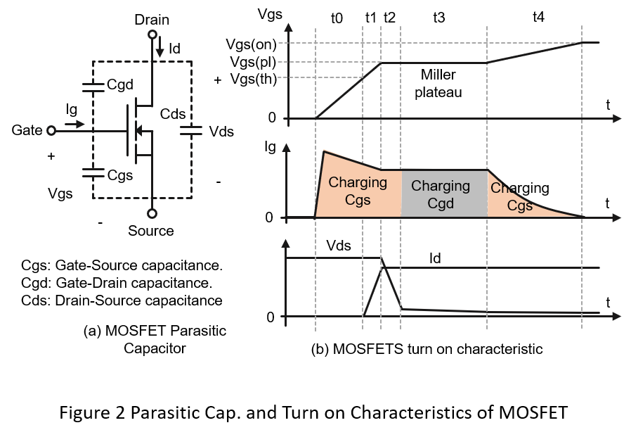
Before talking about the turn on step of the switch, it have to know the basic characteristics of the switch. Take N-MOSFET as an example. As shown in Figure 2(a), there are parasitic capacitances in the gate, drain, and source of the MOSFET. In the datasheet of MOSFET, it will show three parameters Ciss, Crss and Coss as the parasitic capacitances like Table 1.
- Ciss is the MOSFET Gate input capacitance, which is the sum of Cgs and Cgd. When turn on the MOSFET, it needed to charge the Ciss first. The total energy for turn on the MOSFET is Qgate.
- Coss is the MOSFET Gate output capacitance, which is the sum of Cds and Cgs. When turn off the MOSFET, it needed to discharge the energy of Coss.
- Crss reverse transfer capacitance. If Crss is large, it will slow down the MOSFET switching speed. The charge energy is Qgd.
| Capacitances | Designation | |
| Ciss | Cgs+Cgd | Input capacitance |
| Crss | Cgd | Reverse transfer capacitance |
| Coss | Cds+Cgd | Output capacitance |
- Ciss is the MOSFET Gate input capacitance, which is the sum of Cgs and Cgd. When turn on the MOSFET, it needed to charge the Ciss first. The total energy for turn on the MOSFET is Qgate.
- Coss is the MOSFET Gate output capacitance, which is the sum of Cds and Cgs. When turn off the MOSFET, it needed to discharge the energy of Coss.
- Crss reverse transfer capacitance. If Crss is large, it will slow down the MOSFET switching speed. The charge energy is Qgd.
Figure 2(b) is a simple MOSFET turn on diagram, which can basically divided into 5 stages.
- t0: The control signal charges the Cgs. Vgs still below Vgs(th), the MOSFET has not been turn on.
- t1: The control signal continues to charge the Cgs. As soon as Vgs passes Vgs(th), the MOSFET turn-on process starts.
- t2: The control signal continues to charge the Cgs, the Vgs maintains Vgs(pl). At this stage, Vds voltage will drops rapidly.
- t3: The control signal charges the Cgd, and the Vgs still remains at Vgs(pl). At this time, Vds is decreasing to reach on-state.
- t4: The control signal charges Cgs, and the Vgs voltage is greater than Vgs(pl), and the MOSFET is fully turned on.
During the MOSFET turn on stage, it needed to charge the Cgs and Cgd separately. And the total energy is Qgate. The MOSFET turn off stage is reverse direction of turn on. The energy in the input capacitor (Ciss) must be removed.
2. Common Gate Driver Voltage
Table 2 shows the common gate drive voltages of IGBT and MOSFET (Si, Sic, GaN). The positive voltage of the gate drive should be high enough to ensure that the gate is fully turned on. Also need to make sure drive voltage not to exceed the maximum gate voltage.
Si-MOSFET typical using +12 to drive, +15V is commonly used to drive IGBT or SiC, and the gate voltage for GaN is +5V.
When the gate voltage is 0V, it can meet the turn off condition for all device. However, a negative voltage is often applied. It can accelerate the turn off stage, also can avoid the device turn on by noise.
In gate driver applications, there are parasitic inductance and capacitance between a switch and the driver reference. When the switch is turn off, the parasitic inductance may cause a gate source voltage. The Vgs(th) for IGBTs is a few volts, typically 3V. But MOSFET, SiC and GaN can be as low as a 1volt. If there is a noise exceeding 1V, it will have a chance to turn on, causing the high low side switch short circuit, which may cause damage to the switch. Therefore, an appropriate negative drive voltage ensures that the gate source is always actually zero or less.
| IGBT | Si-MOSFET | SiC | GaN | |
| Turn on Vol. | +15V | +10V to 20V | +15V to 20V | +5V to +6V |
| Turn off Vol. | -5V to -15V | 0V to -2V | -2V to -5V | 0V to -3V |
| Common Drive Voltage | +15V/-9V | +12V/0V | +15V/-3V | +5V/0V |
| +15V/-5V | - | +15V/-5V | +6V/-3V |
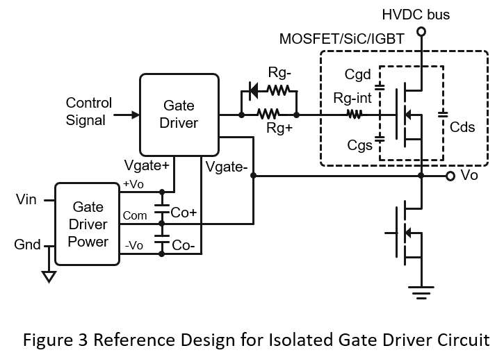
3. Reference Design Circuit and Calculation
Figure 3 shows a reference design for isolated driver, which is composed by isolated gate driver, isolated power supply, and switch device. The first step for design the gate driver circuit is to confirm the specifications of the switching elements, then the drive current capability of the isolated gate driver, and finally select a suitable isolated power supply.
Rg: Between the isolation driver and the switch gate, a resistor is usually connected in series to limit the turn on speed. The calculation method is as follows:
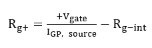
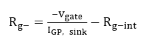
IGP, source and IGP, sink Is the drive and sink current of the isolated driver.
Rg-int Internal gate resistance of switch device.
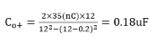
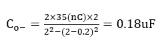
Co: The output capacitance of the isolated power supply is mainly used to provide the drive current of the isolated driver. The calculation method is as follows:
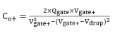
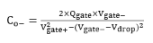
Qgate The total gate charge of switch device.
Vgate, Vgate- The positive and negative output voltage of isolated power supply
Vdrop Estimated output voltage drop
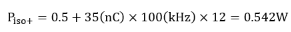
Piso: Output power of Isolated power supply, Provide power to isolated driver and to turn on and off the switch
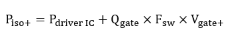
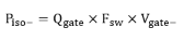
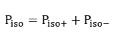
Pdriver IC Power consumption of isolated gate driver
Fsw Switching frequency of the system
4. Example
Example 1 uses Infineon's Si-MOSFET, the model is IPA95R450P7, and uses the reference circuit in Figure 3 to calculate the required parameters
1. The driver and sink current is IGP, source=6A and IGP, sink=4A,Rg-int is 1Ω. The Vgate+=12V, Vgate-=-2V. The Rg+ and Rg- can be calculated
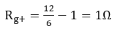
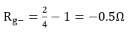
It is recommended Rg+ is more than 1Ω, and Rg- can put 0Ω.
2. Assume the output voltage drop of the isolated converter cannot exceed 0.2V. Qgate is 35 nC, it can calculate the output capacitance
The recommended Co+ and Co- is 0.47uF to 1uF.
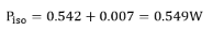
3. Assume the power consumption of the isolated driver is 0.5W, the Qgate of the switch is 35nC, the switching frequency is 100kHz, and the driving voltage is Vgate+=12V, Vgate-=-2V, the converter output power can be calculated
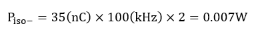
It is recommended to use a 1W isolated converter.
Example 2 uses Infineon's IGBT, the model is AIKW75N60CT, and uses the reference circuit in Figure 3 to calculate the required parameters
1. The driver and sink current is IGP, source=6A and IGP, sink=4A,Rg-int is 0Ω. The Vgate+=15V, Vgate-=-9V. The Rg+ and Rg- can be calculated
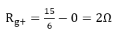
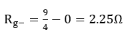
It is recommended Rg+ is more than 2Ω, and Rg- can put 2.25Ω.
2. Assume the output voltage drop of the isolated converter cannot exceed 0.3V. Qgate is 470 nC, it can calculate the output capacitance
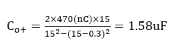
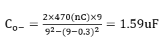
The recommended Co+ and Co- is 2.2uF.
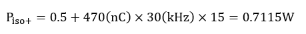
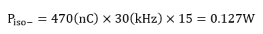
3. Assume the power consumption of the isolated driver is 0.5W, the Qgate of the switch is 470nC, the switching frequency is 30kHz, and the driving voltage is Vgate+=15V, Vgate-=-9V, the converter output power can be calculated
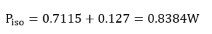
It is recommended to use a 1W to 1.5W isolated converter.
5. Conclusion
Different switching device have suitable driving voltages. Through the above formulas and steps, selecting a suitable driver can calculate the gate resistance, converter output capacitance and converter output power. It is still need to pay attention to the corresponding specifications for different application. For example, in motor driver application. The insulation requirement must be taking into considered. It can refer to standard of IEC 61800.
CTC is a professional service provider for high-end power supply modules (AC to DC Converter and DC to DC Converter) for critical applications worldwide since 30 years. Our core competence is to design and deliver products with leading technologies, competitive pricing, extremely flexible lead-time, global technical service and high-quality manufacturing (Made In Taiwan).
CTC is the only corporation certificated with ISO-9001, IATF-16949, ISO22613(IRIS), and ESD/ANSI-2020. We can 100% ensure not only the product, but also our workflow and service to match quality management system for every high-end application from the very beginning. From design to manufacturing and technical support, every single detail is operated under highest standard.